- 您现在的位置:买卖IC网 > Sheet目录364 > SST25VF064C-80-4I-Q2AE-T (Microchip Technology)IC FLASH SER 64M DUAL I/O 8WSON
�� �
�
�64� Mbit� SPI� Serial� Dual� I/O� Flash�
�A� Microchip� Technology� Company�
�SST25VF064C�
�Data� Sheet�
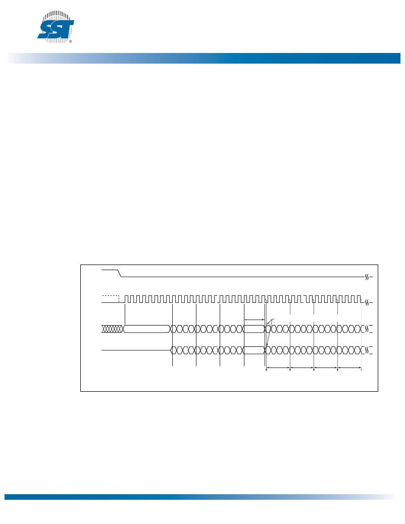
�Fast-Read� Dual� I/O� (50� MHz)�
�The� Fast-Read� Dual� I/O� (BBH)� instruction� reduces� the� total� number� of� input� clock� cycles,� which� results�
�in� faster� data� access.� The� device� is� first� selected� by� driving� Chip� Enable� CE#� low.� Fast-Read� Dual� I/O�
�is� initiated� by� executing� an� 8-bit� command� (BBH)� on� SI/SIO� 0� ,� thereafter,� the� device� accepts� address�
�bits� A23-A0� and� a� dummy� byte� on� SI/SIO� 0� and� SO/SIO� 1� .� It� offers� the� capability� to� input� address� bits�
�A23-A0� at� a� rate� of� two� bits� per� clock.� Odd� address� bits� A23� through� A1� are� input� on� SIO� 1� and� even�
�address� bits� A22� through� A0� are� input� on� SIO� 0� ,� alternately� For� example� the� most� significant� bit� is� input�
�first� followed� by� A23/22,� A21/A20,� and� so� on.� Each� bit� is� latched� at� the� same� rising� edge� of� the� Serial�
�Clock� (SCK).� The� input� data� during� the� dummy� clocks� is� “don’t� care”.� However,� the� SIO� 0� and� SIO� 1� pin�
�must� be� in� high-impedance� prior� to� the� falling� edge� of� the� first� data� output� clock.�
�Following� a� dummy� cycle,� the� Fast-Read� Dual� I/O� instruction� outputs� the� data� starting� from� the� speci-�
�fied� address� location� on� the� SIO� 1� and� SIO� 0� lines.� SIO� 1� outputs,� per� clock� sequence,� odd� data� bits� D7,�
�D5,� D3,� and� D1;� and� SIO� 0� outputs� even� data� bits� D6,� D4,� D2,� and� D0� per� clock� edge.� CE#� must� remain�
�active� low� for� the� duration� of� the� Fast-Read� Dual� I/O� instruction� cycle.� The� data� output� stream� is� con-�
�tinuous� through� all� addresses� until� terminated� by� a� low-to-high� transition� on� CE#.�
�The� internal� address� pointer� will� automatically� increment� until� the� highest� memory� address� is� reached.�
�Once� the� highest� memory� address� is� reached,� the� address� pointer� automatically� increments� to� the�
�beginning� (wraparound)� of� the� address� space.� For� example,� once� the� data� from� address� location�
�7FFFFFH� is� read,� the� next� output� is� from� address� location� 000000H.� See� Figure� 9� for� the� Fast-Read�
�Dual� I/o� sequence.�
�CE#�
�MODE� 3�
�0� 1� 2� 3� 4� 5� 6� 7� 8� 9� 10� 11� 12� 13� 14� 15� 16� 17� 18� 19� 20� 21� 22� 23� 24� 25� 26� 27� 28� 29� 30� 31� 32� 33� 34� 35� 36� 37� 38� 39�
�SCK�
�MODE� 0�
�Dummy�
�Cycle�
�IO,� Switches� from� Input� to� Output�
�SIO0�
�BB�
�6� 4� 2� 0� 6� 4� 2� 0� 6� 4� 2� 0�
�X�
�6� 4� 2� 0� 6� 4� 2� 0� 6� 4� 2� 0� 6� 4� 2� 0� 6�
�DOUT�
�DOUT�
�DOUT�
�DOUT�
�SIO1�
�7� 5� 3� 1�
�7� 5� 3� 1�
�7� 5� 3� 1�
�X�
�7� 5� 3� 1�
�7� 5� 3� 1�
�7� 5� 3� 1�
�7� 5� 3� 1� 7�
�MSB�
�MSB�
�MSB�
�MSB�
�A23-16�
�A15-8�
�A7-0�
�N�
�N+1�
�N+2�
�N+3�
�1392� F29.0�
�Figure� 9:� Fast-Read� Dual� I/O� Sequence�
�?2011� Silicon� Storage� Technology,� Inc.�
�15�
�DS25036A�
�06/11�
�发布紧急采购,3分钟左右您将得到回复。
相关PDF资料
SST25VF080B-80-4I-QAE-T
IC FLASH SER 8MB 50MHZ SPI 8WSON
SST25VF512-20-4C-SAE-T
IC FLASH SER 512K 20MHZ 8SOIC
SST25VF512A-33-4I-QAE-T
IC FLASH SER 512KB 33MHZ 8WSON
SST25WF040-40-5I-QAE-T
IC FLASH SER 4MB 40MHZ SPI 8WSON
SST25WF080-75-4I-ZAE
IC FLSH SER 8MB 75MHZ SPI 8CSP
SST26VF032A-80-5I-S2AE
IC FLASH 32MBIT 8SOIC
SST38VF6402-90-5I-B3KE-T
IC FLASH MPF 64MBIT 90NS 48TFBGA
SST39LF802C-55-4C-MAQE-T
IC FLASH MPF 8MBIT 48-WFBGA
相关代理商/技术参数
SST25VF064C-80-4I-Q2CE
制造商:SST 制造商全称:Silicon Storage Technology, Inc 功能描述:64 Mbit SPI Serial Dual I/O Flash
SST25VF064C804IS3AE
制造商:Microchip Technology Inc 功能描述:
SST25VF064C-80-4I-S3AE
功能描述:闪存 64M (8Mx8) 80MHz Industrial Temp RoHS:否 制造商:ON Semiconductor 数据总线宽度:1 bit 存储类型:Flash 存储容量:2 MB 结构:256 K x 8 定时类型: 接口类型:SPI 访问时间: 电源电压-最大:3.6 V 电源电压-最小:2.3 V 最大工作电流:15 mA 工作温度:- 40 C to + 85 C 安装风格:SMD/SMT 封装 / 箱体: 封装:Reel
SST25VF064C-80-4I-S3AE_
制造商:Microchip Technology Inc 功能描述:
SST25VF064C-80-4I-S3AE-T
功能描述:闪存 2.7V to 3.6V 64Mbit SPI Serial 闪存 RoHS:否 制造商:ON Semiconductor 数据总线宽度:1 bit 存储类型:Flash 存储容量:2 MB 结构:256 K x 8 定时类型: 接口类型:SPI 访问时间: 电源电压-最大:3.6 V 电源电压-最小:2.3 V 最大工作电流:15 mA 工作温度:- 40 C to + 85 C 安装风格:SMD/SMT 封装 / 箱体: 封装:Reel
SST25VF064C-80-4I-S3CE
制造商:SST 制造商全称:Silicon Storage Technology, Inc 功能描述:64 Mbit SPI Serial Dual I/O Flash
SST25VF064C-80-4I-SAE
制造商:SST 制造商全称:Silicon Storage Technology, Inc 功能描述:64 Mbit SPI Serial Dual I/O Flash
SST25VF064C804ISCE
制造商:Microchip Technology Inc 功能描述: